Subscribe

RSS Feed (xml)

Powered By

Skin Design:
Free Blogger Skins

Powered by Blogger


Showing posts with label DIODES AND RECTIFIERS 3C3. Show all posts

Tuesday, September 2, 2008

Introduction DIODES AND RECTIFIERS


A diode is an electrical device allowing current to move through it in one direction with far greater ease than in the other. The most common kind of diode in modern circuit design is the semiconductor diode, although other diode technologies exist. Semiconductor diodes are symbolized in schematic diagrams such as Figure below. The term “diode” is customarily reserved for small signal devices, I ≤ 1 A. The term rectifier is used for power devices, I > 1 A.

Semiconductor diode schematic symbol: Arrows indicate the direction of electron current flow.

When placed in a simple battery-lamp circuit, the diode will either allow or prevent current through the lamp, depending on the polarity of the applied voltage. (Figure below)

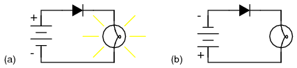
Diode operation: (a) Current flow is permitted; the diode is forward biased. (b) Current flow is prohibited; the diode is reversed biased.

When the polarity of the battery is such that electrons are allowed to flow through the diode, the diode is said to be forward-biased. Conversely, when the battery is “backward” and the diode blocks current, the diode is said to be reverse-biased. A diode may be thought of as like a switch: “closed” when forward-biased and “open” when reverse-biased.

Oddly enough, the direction of the diode symbol's “arrowhead” points against the direction of electron flow. This is because the diode symbol was invented by engineers, who predominantly use conventional flow notation in their schematics, showing current as a flow of charge from the positive (+) side of the voltage source to the negative (-). This convention holds true for all semiconductor symbols possessing “arrowheads:” the arrow points in the permitted direction of conventional flow, and against the permitted direction of electron flow.

Diode behavior is analogous to the behavior of a hydraulic device called a check valve. A check valve allows fluid flow through it in only one direction as in Figure below.

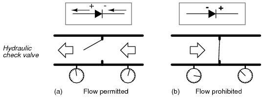
Hydraulic check valve analogy: (a) Electron current flow permitted. (b) Current flow prohibited.

Check valves are essentially pressure-operated devices: they open and allow flow if the pressure across them is of the correct “polarity” to open the gate (in the analogy shown, greater fluid pressure on the right than on the left). If the pressure is of the opposite “polarity,” the pressure difference across the check valve will close and hold the gate so that no flow occurs.

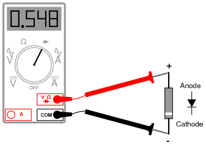
Like check valves, diodes are essentially “pressure-” operated (voltage-operated) devices. The essential difference between forward-bias and reverse-bias is the polarity of the voltage dropped across the diode. Let's take a closer look at the simple battery-diode-lamp circuit shown earlier, this time investigating voltage drops across the various components in Figure below.

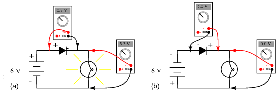
Diode circuit voltage measurements: (a) Forward biased. (b) Reverse biased.

A forward-biased diode conducts current and drops a small voltage across it, leaving most of the battery voltage dropped across the lamp. If the battery's polarity is reversed, the diode becomes reverse-biased, and drops all of the battery's voltage leaving none for the lamp. If we consider the diode to be a self-actuating switch (closed in the forward-bias mode and open in the reverse-bias mode), this behavior makes sense. The most substantial difference is that the diode drops a lot more voltage when conducting than the average mechanical switch (0.7 volts versus tens of millivolts).

This forward-bias voltage drop exhibited by the diode is due to the action of the depletion region formed by the P-N junction under the influence of an applied voltage. If no voltage applied is across a semiconductor diode, a thin depletion region exists around the region of the P-N junction, preventing current flow. (Figure below (a)) The depletion region is almost devoid of available charge carriers, and acts as an insulator:

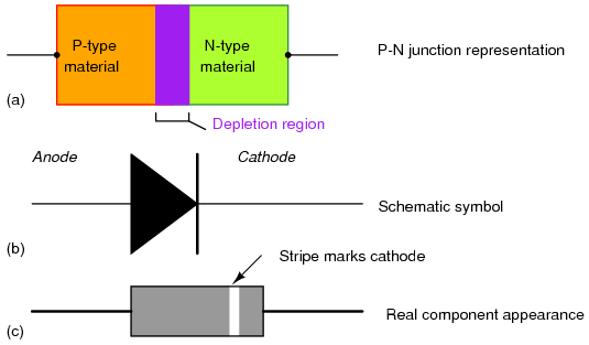
Diode representations: PN-junction model, schematic symbol, physical part.

The schematic symbol of the diode is shown in Figure above (b) such that the anode (pointing end) corresponds to the P-type semiconductor at (a). The cathode bar, non-pointing end, at (b) corresponds to the N-type material at (a). Also note that the cathode stripe on the physical part (c) corresponds to the cathode on the symbol.

If a reverse-biasing voltage is applied across the P-N junction, this depletion region expands, further resisting any current through it. (Figure below)

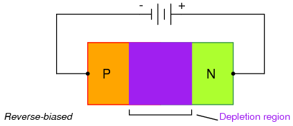
Depletion region expands with reverse bias.

Conversely, if a forward-biasing voltage is applied across the P-N junction, the depletion region collapses becoming thinner. The diode becomes less resistive to current through it. In order for a sustained current to go through the diode; though, the depletion region must be fully collapsed by the applied voltage. This takes a certain minimum voltage to accomplish, called the forward voltage as illustrated in Figure below.

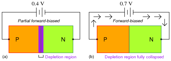
Inceasing forward bias from (a) to (b) decreases depletion region thickness.

For silicon diodes, the typical forward voltage is 0.7 volts, nominal. For germanium diodes, the forward voltage is only 0.3 volts. The chemical constituency of the P-N junction comprising the diode accounts for its nominal forward voltage figure, which is why silicon and germanium diodes have such different forward voltages. Forward voltage drop remains approximately constant for a wide range of diode currents, meaning that diode voltage drop is not like that of a resistor or even a normal (closed) switch. For most simplified circuit analysis, the voltage drop across a conducting diode may be considered constant at the nominal figure and not related to the amount of current.

Actually, forward voltage drop is more complex. An equation describes the exact current through a diode, given the voltage dropped across the junction, the temperature of the junction, and several physical constants. It is commonly known as the diode equation:

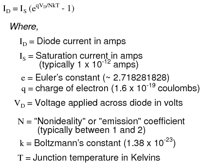
The term kT/q describes the voltage produced within the P-N junction due to the action of temperature, and is called the thermal voltage, or Vt of the junction. At room temperature, this is about 26 millivolts. Knowing this, and assuming a “nonideality” coefficient of 1, we may simplify the diode equation and re-write it as such:

You need not be familiar with the “diode equation” to analyze simple diode circuits. Just understand that the voltage dropped across a current-conducting diode does change with the amount of current going through it, but that this change is fairly small over a wide range of currents. This is why many textbooks simply say the voltage drop across a conducting, semiconductor diode remains constant at 0.7 volts for silicon and 0.3 volts for germanium. However, some circuits intentionally make use of the P-N junction's inherent exponential current/voltage relationship and thus can only be understood in the context of this equation. Also, since temperature is a factor in the diode equation, a forward-biased P-N junction may also be used as a temperature-sensing device, and thus can only be understood if one has a conceptual grasp on this mathematical relationship.

A reverse-biased diode prevents current from going through it, due to the expanded depletion region. In actuality, a very small amount of current can and does go through a reverse-biased diode, called the leakage current, but it can be ignored for most purposes. The ability of a diode to withstand reverse-bias voltages is limited, as it is for any insulator. If the applied reverse-bias voltage becomes too great, the diode will experience a condition known as breakdown (Figure below), which is usually destructive. A diode's maximum reverse-bias voltage rating is known as the Peak Inverse Voltage, or PIV, and may be obtained from the manufacturer. Like forward voltage, the PIV rating of a diode varies with temperature, except that PIV increases with increased temperature and decreases as the diode becomes cooler -- exactly opposite that of forward voltage.

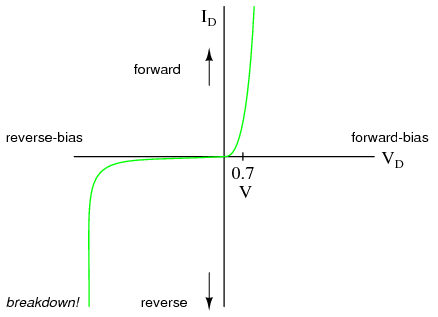
Diode curve: showing knee at 0.7 V forward bias for Si, and reverse breakdown.

Typically, the PIV rating of a generic “rectifier” diode is at least 50 volts at room temperature. Diodes with PIV ratings in the many thousands of volts are available for modest prices.

  • REVIEW:
  • A diode is an electrical component acting as a one-way valve for current.
  • When voltage is applied across a diode in such a way that the diode allows current, the diode is said to be forward-biased.
  • When voltage is applied across a diode in such a way that the diode prohibits current, the diode is said to be reverse-biased.
  • The voltage dropped across a conducting, forward-biased diode is called the forward voltage. Forward voltage for a diode varies only slightly for changes in forward current and temperature, and is fixed by the chemical composition of the P-N junction.
  • Silicon diodes have a forward voltage of approximately 0.7 volts.
  • Germanium diodes have a forward voltage of approximately 0.3 volts.
  • The maximum reverse-bias voltage that a diode can withstand without “breaking down” is called the Peak Inverse Voltage, or PIV rating.

Meter check of a diode DIODES AND RECTIFIERS


Being able to determine the polarity (cathode versus anode) and basic functionality of a diode is a very important skill for the electronics hobbyist or technician to have. Since we know that a diode is essentially nothing more than a one-way valve for electricity, it makes sense we should be able to verify its one-way nature using a DC (battery-powered) ohmmeter as in Figure below. Connected one way across the diode, the meter should show a very low resistance at (a). Connected the other way across the diode, it should show a very high resistance at (b) (“OL” on some digital meter models).

Determination of diode polarity: (a) Low resistance indicates forward bias, black lead is cathode and red lead anode (for most meters) (b) Reversing leads shows high resistance indicating reverse bias.

Of course, to determine which end of the diode is the cathode and which is the anode, you must know with certainty which test lead of the meter is positive (+) and which is negative (-) when set to the “resistance” or “Ω” function. With most digital multimeters I've seen, the red lead becomes positive and the black lead negative when set to measure resistance, in accordance with standard electronics color-code convention. However, this is not guaranteed for all meters. Many analog multimeters, for example, actually make their black leads positive (+) and their red leads negative (-) when switched to the “resistance” function, because it is easier to manufacture it that way!

One problem with using an ohmmeter to check a diode is that the readings obtained only have qualitative value, not quantitative. In other words, an ohmmeter only tells you which way the diode conducts; the low-value resistance indication obtained while conducting is useless. If an ohmmeter shows a value of “1.73 ohms” while forward-biasing a diode, that figure of 1.73 Ω doesn't represent any real-world quantity useful to us as technicians or circuit designers. It neither represents the forward voltage drop nor any “bulk” resistance in the semiconductor material of the diode itself, but rather is a figure dependent upon both quantities and will vary substantially with the particular ohmmeter used to take the reading.

For this reason, some digital multimeter manufacturers equip their meters with a special “diode check” function which displays the actual forward voltage drop of the diode in volts, rather than a “resistance” figure in ohms. These meters work by forcing a small current through the diode and measuring the voltage dropped between the two test leads. (Figure below)

Meter with a “Diode check” function displays the forward voltage drop of 0.548 volts instead of a low resistance.

The forward voltage reading obtained with such a meter will typically be less than the “normal” drop of 0.7 volts for silicon and 0.3 volts for germanium, because the current provided by the meter is of trivial proportions. If a multimeter with diode-check function isn't available, or you would like to measure a diode's forward voltage drop at some non-trivial current, the circuit of Figure below may be constructed using a battery, resistor, and voltmeter

Measuring forward voltage of a diode without“diode check” meter function: (a) Schematic diagram. (b) Pictorial diagram.

Connecting the diode backwards to this testing circuit will simply result in the voltmeter indicating the full voltage of the battery.

If this circuit were designed to provide a constant or nearly constant current through the diode despite changes in forward voltage drop, it could be used as the basis of a temperature-measurement instrument, the voltage measured across the diode being inversely proportional to diode junction temperature. Of course, diode current should be kept to a minimum to avoid self-heating (the diode dissipating substantial amounts of heat energy), which would interfere with temperature measurement.

Beware that some digital multimeters equipped with a “diode check” function may output a very low test voltage (less than 0.3 volts) when set to the regular “resistance” (Ω) function: too low to fully collapse the depletion region of a PN junction. The philosophy here is that the “diode check” function is to be used for testing semiconductor devices, and the “resistance” function for anything else. By using a very low test voltage to measure resistance, it is easier for a technician to measure the resistance of non-semiconductor components connected to semiconductor components, since the semiconductor component junctions will not become forward-biased with such low voltages.

Consider the example of a resistor and diode connected in parallel, soldered in place on a printed circuit board (PCB). Normally, one would have to unsolder the resistor from the circuit (disconnect it from all other components) before measuring its resistance, otherwise any parallel-connected components would affect the reading obtained. When using a multimeter which outputs a very low test voltage to the probes in the “resistance” function mode, the diode's PN junction will not have enough voltage impressed across it to become forward-biased, and will only pass negligible current. Consequently, the meter “sees” the diode as an open (no continuity), and only registers the resistor's resistance. (Figure below)

Ohmmeter equipped with a low test voltage (<0.7>

If such an ohmmeter were used to test a diode, it would indicate a very high resistance (many mega-ohms) even if connected to the diode in the “correct” (forward-biased) direction. (Figure below)

Ohmmeter equipped with a low test voltage, too low to forward bias diodes, does not see diodes.

Reverse voltage strength of a diode is not as easily tested, because exceeding a normal diode's PIV usually results in destruction of the diode. Special types of diodes, though, which are designed to “break down” in reverse-bias mode without damage (called zener diodes), which are tested with the same voltage source / resistor / voltmeter circuit, provided that the voltage source is of high enough value to force the diode into its breakdown region. More on this subject in a later section of this chapter.

  • REVIEW:
  • An ohmmeter may be used to qualitatively check diode function. There should be low resistance measured one way and very high resistance measured the other way. When using an ohmmeter for this purpose, be sure you know which test lead is positive and which is negative! The actual polarity may not follow the colors of the leads as you might expect, depending on the particular design of meter.
  • Some multimeters provide a “diode check” function that displays the actual forward voltage of the diode when it's conducting current. Such meters typically indicate a slightly lower forward voltage than what is “nominal” for a diode, due to the very small amount of current used during the check.

Diode ratings DIODES AND RECTIFIERS


In addition to forward voltage drop (Vf) and peak inverse voltage (PIV), there are many other ratings of diodes important to circuit design and component selection. Semiconductor manufacturers provide detailed specifications on their products -- diodes included -- in publications known as datasheets. Datasheets for a wide variety of semiconductor components may be found in reference books and on the internet. I prefer the internet as a source of component specifications because all the data obtained from manufacturer websites are up-to-date.

A typical diode datasheet will contain figures for the following parameters:

Maximum repetitive reverse voltage = VRRM, the maximum amount of voltage the diode can withstand in reverse-bias mode, in repeated pulses. Ideally, this figure would be infinite.

Maximum DC reverse voltage = VR or VDC, the maximum amount of voltage the diode can withstand in reverse-bias mode on a continual basis. Ideally, this figure would be infinite.

Maximum forward voltage = VF, usually specified at the diode's rated forward current. Ideally, this figure would be zero: the diode providing no opposition whatsoever to forward current. In reality, the forward voltage is described by the “diode equation.”

Maximum (average) forward current = IF(AV), the maximum average amount of current the diode is able to conduct in forward bias mode. This is fundamentally a thermal limitation: how much heat can the PN junction handle, given that dissipation power is equal to current (I) multiplied by voltage (V or E) and forward voltage is dependent upon both current and junction temperature. Ideally, this figure would be infinite.

Maximum (peak or surge) forward current = IFSM or if(surge), the maximum peak amount of current the diode is able to conduct in forward bias mode. Again, this rating is limited by the diode junction's thermal capacity, and is usually much higher than the average current rating due to thermal inertia (the fact that it takes a finite amount of time for the diode to reach maximum temperature for a given current). Ideally, this figure would be infinite.

Maximum total dissipation = PD, the amount of power (in watts) allowable for the diode to dissipate, given the dissipation (P=IE) of diode current multiplied by diode voltage drop, and also the dissipation (P=I2R) of diode current squared multiplied by bulk resistance. Fundamentally limited by the diode's thermal capacity (ability to tolerate high temperatures).

Operating junction temperature = TJ, the maximum allowable temperature for the diode's PN junction, usually given in degrees Celsius (oC). Heat is the “Achilles' heel” of semiconductor devices: they must be kept cool to function properly and give long service life.

Storage temperature range = TSTG, the range of allowable temperatures for storing a diode (unpowered). Sometimes given in conjunction with operating junction temperature (TJ), because the maximum storage temperature and the maximum operating temperature ratings are often identical. If anything, though, maximum storage temperature rating will be greater than the maximum operating temperature rating.

Thermal resistance = R(Θ), the temperature difference between junction and outside air (R(Θ)JA) or between junction and leads (R(Θ)JL) for a given power dissipation. Expressed in units of degrees Celsius per watt (oC/W). Ideally, this figure would be zero, meaning that the diode package was a perfect thermal conductor and radiator, able to transfer all heat energy from the junction to the outside air (or to the leads) with no difference in temperature across the thickness of the diode package. A high thermal resistance means that the diode will build up excessive temperature at the junction (where it's critical) despite best efforts at cooling the outside of the diode, and thus will limit its maximum power dissipation.

Maximum reverse current = IR, the amount of current through the diode in reverse-bias operation, with the maximum rated inverse voltage applied (VDC). Sometimes referred to as leakage current. Ideally, this figure would be zero, as a perfect diode would block all current when reverse-biased. In reality, it is very small compared to the maximum forward current.

Typical junction capacitance = CJ, the typical amount of capacitance intrinsic to the junction, due to the depletion region acting as a dielectric separating the anode and cathode connections. This is usually a very small figure, measured in the range of picofarads (pF).

Reverse recovery time = trr, the amount of time it takes for a diode to “turn off” when the voltage across it alternates from forward-bias to reverse-bias polarity. Ideally, this figure would be zero: the diode halting conduction immediately upon polarity reversal. For a typical rectifier diode, reverse recovery time is in the range of tens of microseconds; for a “fast switching” diode, it may only be a few nanoseconds.

Most of these parameters vary with temperature or other operating conditions, and so a single figure fails to fully describe any given rating. Therefore, manufacturers provide graphs of component ratings plotted against other variables (such as temperature), so that the circuit designer has a better idea of what the device is capable of.

Rectifier circuits DIODES AND RECTIFIERS


Now we come to the most popular application of the diode: rectification. Simply defined, rectification is the conversion of alternating current (AC) to direct current (DC). This involves a device that only allows one-way flow of electrons. As we have seen, this is exactly what a semiconductor diode does. The simplest kind of rectifier circuit is the half-wave rectifier. It only allows one half of an AC waveform to pass through to the load. (Figure below)

Half-wave rectifier circuit.

For most power applications, half-wave rectification is insufficient for the task. The harmonic content of the rectifier's output waveform is very large and consequently difficult to filter. Furthermore, the AC power source only supplies power to the load once every half-cycle, meaning that much of its capacity is unused. Half-wave rectification is, however, a very simple way to reduce power to a resistive load. Some two-position lamp dimmer switches apply full AC power to the lamp filament for “full” brightness and then half-wave rectify it for a lesser light output. (Figure below)

Half-wave rectifier application: Two level lamp dimmer.

In the “Dim” switch position, the incandescent lamp receives approximately one-half the power it would normally receive operating on full-wave AC. Because the half-wave rectified power pulses far more rapidly than the filament has time to heat up and cool down, the lamp does not blink. Instead, its filament merely operates at a lesser temperature than normal, providing less light output. This principle of “pulsing” power rapidly to a slow-responding load device to control the electrical power sent to it is common in the world of industrial electronics. Since the controlling device (the diode, in this case) is either fully conducting or fully nonconducting at any given time, it dissipates little heat energy while controlling load power, making this method of power control very energy-efficient. This circuit is perhaps the crudest possible method of pulsing power to a load, but it suffices as a proof-of-concept application.

If we need to rectify AC power to obtain the full use of both half-cycles of the sine wave, a different rectifier circuit configuration must be used. Such a circuit is called a full-wave rectifier. One kind of full-wave rectifier, called the center-tap design, uses a transformer with a center-tapped secondary winding and two diodes, as in Figure below.

Full-wave rectifier, center-tapped design.

This circuit's operation is easily understood one half-cycle at a time. Consider the first half-cycle, when the source voltage polarity is positive (+) on top and negative (-) on bottom. At this time, only the top diode is conducting; the bottom diode is blocking current, and the load “sees” the first half of the sine wave, positive on top and negative on bottom. Only the top half of the transformer's secondary winding carries current during this half-cycle as in Figure below.

Full-wave center-tap rectifier: Top half of secondary winding conducts during positive half-cycle of input, delivering positive half-cycle to load..

During the next half-cycle, the AC polarity reverses. Now, the other diode and the other half of the transformer's secondary winding carry current while the portions of the circuit formerly carrying current during the last half-cycle sit idle. The load still “sees” half of a sine wave, of the same polarity as before: positive on top and negative on bottom. (Figure below)

Full-wave center-tap rectifier: During negative input half-cycle, bottom half of secondary winding conducts, delivering a positive half-cycle to the load.

One disadvantage of this full-wave rectifier design is the necessity of a transformer with a center-tapped secondary winding. If the circuit in question is one of high power, the size and expense of a suitable transformer is significant. Consequently, the center-tap rectifier design is only seen in low-power applications.

The full-wave center-tapped rectifier polarity at the load may be reversed by changing the direction of the diodes. Furthermore, the reversed diodes can be paralleled with an existing positive-output rectifier. The result is dual-polarity full-wave center-tapped rectifier in Figure below. Note that the connectivity of the diodes themselves is the same configuration as a bridge.

Dual polarity full-wave center tap rectifier

Another, more popular full-wave rectifier design exists, and it is built around a four-diode bridge configuration. For obvious reasons, this design is called a full-wave bridge. (Figure below)

Full-wave bridge rectifier.

Current directions for the full-wave bridge rectifier circuit are as shown in Figure below for positive half-cycle and Figure below for negative half-cycles of the AC source waveform. Note that regardless of the polarity of the input, the current flows in the same direction through the load. That is, the negative half-cycle of source is a positive half-cycle at the load. The current flow is through two diodes in series for both polarities. Thus, two diode drops of the source voltage are lost (0.7·2=1.4 V for Si) in the diodes. This is a disadvantage compared with a full-wave center-tap design. This disadvantage is only a problem in very low voltage power supplies.

Full-wave bridge rectifier: Electron flow for positive half-cycles.

Full-wave bridge rectifier: Electron flow for negative half=cycles.

Remembering the proper layout of diodes in a full-wave bridge rectifier circuit can often be frustrating to the new student of electronics. I've found that an alternative representation of this circuit is easier both to remember and to comprehend. It's the exact same circuit, except all diodes are drawn in a horizontal attitude, all “pointing” the same direction. (Figure below)

Alternative layout style for Full-wave bridge rectifier.

One advantage of remembering this layout for a bridge rectifier circuit is that it expands easily into a polyphase version in Figure below.

Three-phase full-wave bridge rectifier circuit.

Each three-phase line connects between a pair of diodes: one to route power to the positive (+) side of the load, and the other to route power to the negative (-) side of the load. Polyphase systems with more than three phases are easily accommodated into a bridge rectifier scheme. Take for instance the six-phase bridge rectifier circuit in Figure below.

Six-phase full-wave bridge rectifier circuit.

When polyphase AC is rectified, the phase-shifted pulses overlap each other to produce a DC output that is much “smoother” (has less AC content) than that produced by the rectification of single-phase AC. This is a decided advantage in high-power rectifier circuits, where the sheer physical size of filtering components would be prohibitive but low-noise DC power must be obtained. The diagram in Figure below shows the full-wave rectification of three-phase AC.

Three-phase AC and 3-phase full-wave rectifier output.

In any case of rectification -- single-phase or polyphase -- the amount of AC voltage mixed with the rectifier's DC output is called ripple voltage. In most cases, since “pure” DC is the desired goal, ripple voltage is undesirable. If the power levels are not too great, filtering networks may be employed to reduce the amount of ripple in the output voltage.

Sometimes, the method of rectification is referred to by counting the number of DC “pulses” output for every 360o of electrical “rotation.” A single-phase, half-wave rectifier circuit, then, would be called a 1-pulse rectifier, because it produces a single pulse during the time of one complete cycle (360o) of the AC waveform. A single-phase, full-wave rectifier (regardless of design, center-tap or bridge) would be called a 2-pulse rectifier, because it outputs two pulses of DC during one AC cycle's worth of time. A three-phase full-wave rectifier would be called a 6-pulse unit.

Modern electrical engineering convention further describes the function of a rectifier circuit by using a three-field notation of phases, ways, and number of pulses. A single-phase, half-wave rectifier circuit is given the somewhat cryptic designation of 1Ph1W1P (1 phase, 1 way, 1 pulse), meaning that the AC supply voltage is single-phase, that current on each phase of the AC supply lines moves in only one direction (way), and that there is a single pulse of DC produced for every 360o of electrical rotation. A single-phase, full-wave, center-tap rectifier circuit would be designated as 1Ph1W2P in this notational system: 1 phase, 1 way or direction of current in each winding half, and 2 pulses or output voltage per cycle. A single-phase, full-wave, bridge rectifier would be designated as 1Ph2W2P: the same as for the center-tap design, except current can go both ways through the AC lines instead of just one way. The three-phase bridge rectifier circuit shown earlier would be called a 3Ph2W6P rectifier.

Is it possible to obtain more pulses than twice the number of phases in a rectifier circuit? The answer to this question is yes: especially in polyphase circuits. Through the creative use of transformers, sets of full-wave rectifiers may be paralleled in such a way that more than six pulses of DC are produced for three phases of AC. A 30o phase shift is introduced from primary to secondary of a three-phase transformer when the winding configurations are not of the same type. In other words, a transformer connected either Y-Δ or Δ-Y will exhibit this 30o phase shift, while a transformer connected Y-Y or Δ-Δ will not. This phenomenon may be exploited by having one transformer connected Y-Y feed a bridge rectifier, and have another transformer connected Y-Δ feed a second bridge rectifier, then parallel the DC outputs of both rectifiers. (Figure below) Since the ripple voltage waveforms of the two rectifiers' outputs are phase-shifted 30o from one another, their superposition results in less ripple than either rectifier output considered separately: 12 pulses per 360o instead of just six:

Polyphase rectifier circuit: 3-phase 2-way 12-pulse (3Ph2W12P)

  • REVIEW:
  • Rectification is the conversion of alternating current (AC) to direct current (DC).
  • A half-wave rectifier is a circuit that allows only one half-cycle of the AC voltage waveform to be applied to the load, resulting in one non-alternating polarity across it. The resulting DC delivered to the load “pulsates” significantly.
  • A full-wave rectifier is a circuit that converts both half-cycles of the AC voltage waveform to an unbroken series of voltage pulses of the same polarity. The resulting DC delivered to the load doesn't “pulsate” as much.
  • Polyphase alternating current, when rectified, gives a much “smoother” DC waveform (less ripple voltage) than rectified single-phase AC.

Peak detector DIODES AND RECTIFIERS


A peak detector is a series connection of a diode and a capacitor outputting a DC voltage equal to the peak value of the applied AC signal. The circuit is shown in Figure below with the corresponding SPICE net list. An AC voltage source applied to the peak detector, charges the capacitor to the peak of the input. The diode conducts positive “half cycles,” charging the capacitor to the waveform peak. When the input waveform falls below the DC “peak” stored on the capacitor, the diode is reverse biased, blocking current flow from capacitor back to the source. Thus, the capacitor retains the peak value even as the waveform drops to zero. Another view of the peak detector is that it is the same as a half-wave rectifier with a filter capacitor added to the output.


*SPICE 03441.eps
C1 2 0 0.1u
R1 1 3 1.0k
V1 1 0 SIN(0 5 1k)
D1 3 2 diode
.model diode d
.tran 0.01m 50mm
.end

Peak detector: Diode conducts on positive half cycles charging capacitor to the peak voltage (less diode forward drop).

It takes a few cycles for the capacitor to charge to the peak as in Figure below due to the series resistance (RC “time constant”). Why does the capacitor not charge all the way to 5 V? It would charge to 5 V if an “ideal diode” were obtainable. However, the silicon diode has a forward voltage drop of 0.7 V which subtracts from the 5 V peak of the input.

Peak detector: Capacitor charges to peak within a few cycles.

The circuit in Figure above could represent a DC power supply based on a half-wave rectifier. The resistance would be a few Ohms instead of 1 kΩ due to a transformer secondary winding replacing the voltage source and resistor. A larger “filter” capacitor would be used. A power supply based on a 60 Hz source with a filter of a few hundred µF could supply up to 100 mA. Half-wave supplies seldom supply more due to the difficulty of filtering a half-wave.

The peak detector may be combined with other components to build a crystal radio 03442.png.

Clipper circuits DIODES AND RECTIFIERS


A circuit which removes the peak of a waveform is known as a clipper. A negative clipper is shown in Figure below. This schematic diagram was produced with Xcircuit schematic capture program. Xcircuit produced the SPICE net list Figure below, except for the second, and next to last pair of lines which were inserted with a text editor.


*SPICE 03437.eps
* A K ModelName
D1 0 2 diode
R1 2 1 1.0k
V1 1 0 SIN(0 5 1k)
.model diode d
.tran .05m 3m
.end

Clipper: clips negative peak at -0.7 V.

During the positive half cycle of the 5 V peak input, the diode is reversed biased. The diode does not conduct. It is as if the diode were not there. The positive half cycle is unchanged at the output V(2) in Figure below. Since the output positive peaks actually overlays the input sinewave V(1), the input has been shifted upward in the plot for clarity. In Nutmeg, the SPICE display module, the command “plot v(1)+1)” accomplishes this.

V(1)+1 is actually V(1), a 5 Vptp sinewave, offset by 1 V for display clarity. V(2) output is clipped at -0.7 V, by diode D1.

During the negative half cycle of sinewave input of Figure above, the diode is forward biased, that is, conducting. The negative half cycle of the sinewave is shorted out. The negative half cycle of V(2) would be clipped at 0 V for an ideal diode. The waveform is clipped at -0.7 V due to the forward voltage drop of the silicon diode. The spice model defaults to 0.7 V unless parameters in the model statement specify otherwise. Germanium or Schottky diodes clip at lower voltages.

Closer examination of the negative clipped peak (Figure above) reveals that it follows the input for a slight period of time while the sinewave is moving toward -0.7 V. The clipping action is only effective after the input sinewave exceeds -0.7 V. The diode is not conducting for the complete half cycle, though, during most of it.

The addition of an anti-parallel diode to the existing diode in Figure above yields the symmetrical clipper in Figure below.


*SPICE 03438.eps
D1 0 2 diode
D2 2 0 diode
R1 2 1 1.0k
V1 1 0 SIN(0 5 1k)
.model diode d
.tran 0.05m 3m
.end

Symmetrical clipper: Anti-parallel diodes clip both positive and negative peak, leaving a ± 0.7 V output.

Diode D1 clips the negative peak at -0.7 V as before. The additional diode D2 conducts for positive half cycles of the sine wave as it exceeds 0.7 V, the forward diode drop. The remainder of the voltage drops across the series resistor. Thus, both peaks of the input sinewave are clipped in Figure below. The net list is in Figure above

Diode D1 clips at -0.7 V as it conducts during negative peaks. D2 conducts for positive peaks, clipping at 0.7V.

The most general form of the diode clipper is shown in Figure below. For an ideal diode, the clipping occurs at the level of the clipping voltage, V1 and V2. However, the voltage sources have been adjusted to account for the 0.7 V forward drop of the real silicon diodes. D1 clips at 1.3V +0.7V=2.0V when the diode begins to conduct. D2 clips at -2.3V -0.7V=-3.0V when D2 conducts.


*SPICE 03439.eps
V1 3 0 1.3
V2 4 0 -2.3
D1 2 3 diode
D2 4 2 diode
R1 2 1 1.0k
V3 1 0 SIN(0 5 1k)
.model diode d
.tran 0.05m 3m
.end

D1 clips the input sinewave at 2V. D2 clips at -3V.

The clipper in Figure above does not have to clip both levels. To clip at one level with one diode and one voltage source, remove the other diode and source.

The net list is in Figure above. The waveforms in Figure below show the clipping of v(1) at output v(2).

D1 clips the sinewave at 2V. D2 clips at -3V.

There is also a zener diode clipper circuit in the “Zener diode” section. A zener diode replaces both the diode and the DC voltage source.

A practical application of a clipper is to prevent an amplified speech signal from overdriving a radio transmitter in Figure below. Over driving the transmitter generates spurious radio signals which causes interference with other stations. The clipper is a protective measure.

Clipper prevents over driving radio transmitter by voice peaks.

A sinewave may be squared up by overdriving a clipper. Another clipper application is the protection of exposed inputs of integrated circuits. The input of the IC is connected to a pair of diodes as at node “2” of Figure above . The voltage sources are replaced by the power supply rails of the IC. For example, CMOS IC's use 0V and +5 V. Analog amplifiers might use ±12V for the V1 and V2 sources.

  • REVIEW
  • A resistor and diode driven by an AC voltage source clips the signal observed across the diode.
  • A pair of anti-parallel Si diodes clip symmetrically at ±0.7V
  • The grounded end of a clipper diode(s) can be disconnected and wired to a DC voltage to clip at an arbitrary level.
  • A clipper can serve as a protective measure, preventing a signal from exceeding the clip limits.

Clamper circuits DIODES AND RECTIFIERS


The circuits in Figure below are known as clampers or DC restorers. The corresponding netlist is in Figure below. These circuits clamp a peak of a waveform to a specific DC level compared with a capacitively coupled signal which swings about its average DC level (usually 0V). If the diode is removed from the clamper, it defaults to a simple coupling capacitor– no clamping.

What is the clamp voltage? And, which peak gets clamped? In Figure below (a) the clamp voltage is 0 V ignoring diode drop, (more exactly 0.7 V with Si diode drop). In Figure below, the positive peak of V(1) is clamped to the 0 V (0.7 V) clamp level. Why is this? On the first positive half cycle, the diode conducts charging the capacitor left end to +5 V (4.3 V). This is -5 V (-4.3 V) on the right end at V(1,4). Note the polarity marked on the capacitor in Figure below (a). The right end of the capacitor is -5 V DC (-4.3 V) with respect to ground. It also has an AC 5 V peak sinewave coupled across it from source V(4) to node 1. The sum of the two is a 5 V peak sine riding on a - 5 V DC (-4.3 V) level. The diode only conducts on successive positive excursions of source V(4) if the peak V(4) exceeds the charge on the capacitor. This only happens if the charge on the capacitor drained off due to a load, not shown. The charge on the capacitor is equal to the positive peak of V(4) (less 0.7 diode drop). The AC riding on the negative end, right end, is shifted down. The positive peak of the waveform is clamped to 0 V (0.7 V) because the diode conducts on the positive peak.

Clampers: (a) Positive peak clamped to 0 V. (b) Negative peak clamped to 0 V. (c) Negative peak clamped to 5 V.


*SPICE 03443.eps
V1 6 0 5
D1 6 3 diode
C1 4 3 1000p
D2 0 2 diode
C2 4 2 1000p
C3 4 1 1000p
D3 1 0 diode
V2 4 0 SIN(0 5 1k)
.model diode d
.tran 0.01m 5m
.end

V(4) source voltage 5 V peak used in all clampers. V(1) clamper output from Figure above (a). V(1,4) DC voltage on capacitor in Figure (a). V(2) clamper output from Figure (b). V(3) clamper output from Figure (c).

Suppose the polarity of the diode is reversed as in Figure above (b)? The diode conducts on the negative peak of source V(4). The negative peak is clamped to 0 V (-0.7 V). See V(2) in Figure above.

The most general realization of the clamper is shown in Figure above (c) with the diode connected to a DC reference. The capacitor still charges during the negative peak of the source. Note that the polarities of the AC source and the DC reference are series aiding. Thus, the capacitor charges to the sum to the two, 10 V DC (9.3 V). Coupling the 5 V peak sinewave across the capacitor yields Figure above V(3), the sum of the charge on the capacitor and the sinewave. The negative peak appears to be clamped to 5 V DC (4.3V), the value of the DC clamp reference (less diode drop).

Describe the waveform if the DC clamp reference is changed from 5 V to 10 V. The clamped waveform will shift up. The negative peak will be clamped to 10 V (9.3). Suppose that the amplitude of the sine wave source is increased from 5 V to 7 V? The negative peak clamp level will remain unchanged. Though, the amplitude of the sinewave output will increase.

An application of the clamper circuit is as a “DC restorer” in “composite video” circuitry in both television transmitters and receivers. An NTSC (US video standard) video signal “white level” corresponds to minimum (12.5%) transmitted power. The video “black level” corresponds to a high level (75% of transmitter power. There is a “blacker than black level” corresponding to 100% transmitted power assigned to synchronization signals. The NTSC signal contains both video and synchronization pulses. The problem with the composite video is that its average DC level varies with the scene, dark vs light. The video itself is supposed to vary. However, the sync must always peak at 100%. To prevent the sync signals from drifting with changing scenes, a “DC restorer” clamps the top of the sync pulses to a voltage corresponding to 100% transmitter modulation. [ATCO]

  • REVIEW:
  • A capacitively coupled signal alternates about its average DC level (0 V).
  • The signal out of a clamper appears the have one peak clamped to a DC voltage. Example: The negative peak is clamped to 0 VDC, the waveform appears to be shifted upward. The polarity of the diode determines which peak is clamped.
  • An application of a clamper, or DC restorer, is in clamping the sync pulses of composite video to a voltage corresponding to 100% of transmitter power.

Voltage multipliers DIODES AND RECTIFIERS


A voltage multiplier is a specialized rectifier circuit producing an output which is theoretically an integer times the AC peak input, for example, 2, 3, or 4 times the AC peak input. Thus, it is possible to get 200 VDC from a 100 Vpeak AC source using a doubler, 400 VDC from a quadrupler. Any load in a practical circuit will lower these voltages.

A voltage doubler application is a DC power supply capable of using either a 240 VAC or 120 VAC source. The supply uses a switch selected full-wave bridge to produce about 300 VDC from a 240 VAC source. The 120 V position of the switch rewires the bridge as a doubler producing about 300 VDC from the 120 VAC. In both cases, 300 VDC is produced. This is the input to a switching regulator producing lower voltages for powering, say, a personal computer.

The half-wave voltage doubler in Figure below (a) is composed of two circuits: a clamper at (b) and peak detector (half-wave rectifier) in Figure prior, which is shown in modified form in Figure below (c). C2 has been added to a peak detector (half-wave rectifier).

Half-wave voltage doubler (a) is composed of (b) a clamper and (c) a half-wave rectifier.

Referring to Figure above (b), C2 charges to 5 V (4.3 V considering the diode drop) on the negative half cycle of AC input. The right end is grounded by the conducting D2. The left end is charged at the negative peak of the AC input. This is the operation of the clamper.

During the positive half cycle, the half-wave rectifier comes into play at Figure above (c). Diode D2 is out of the circuit since it is reverse biased. C2 is now in series with the voltage source. Note the polarities of the generator and C2, series aiding. Thus, rectifier D1 sees a total of 10 V at the peak of the sinewave, 5 V from generator and 5 V from C2. D1 conducts waveform v(1) (Figure below), charging C1 to the peak of the sine wave riding on 5 V DC (Figure below v(2)). Waveform v(2) is the output of the doubler, which stabilizes at 10 V (8.6 V with diode drops) after a few cycles of sinewave input.


*SPICE 03255.eps
C1 2 0 1000p
D1 1 2 diode
C2 4 1 1000p
D2 0 1 diode
V1 4 0 SIN(0 5 1k)
.model diode d
.tran 0.01m 5m
.end

Voltage doubler: v(4) input. v(1) clamper stage. v(2) half-wave rectifier stage, which is the doubler output.

The full-wave voltage doubler is composed of a pair of series stacked half-wave rectifiers. (Figure below) The corresponding netlist is in Figure below. The bottom rectifier charges C1 on the negative half cycle of input. The top rectifier charges C2 on the positive halfcycle. Each capacitor takes on a charge of 5 V (4.3 V considering diode drop). The output at node 5 is the series total of C1 + C2 or 10 V (8.6 V with diode drops).


*SPICE 03273.eps
*R1 3 0 100k
*R2 5 3 100k
D1 0 2 diode
D2 2 5 diode
C1 3 0 1000p
C2 5 3 1000p
V1 2 3 SIN(0 5 1k)
.model diode d
.tran 0.01m 5m
.end

Full-wave voltage doubler consists of two half-wave rectifiers operating on alternating polarities.

Note that the output v(5) Figure below reaches full value within one cycle of the input v(2) excursion.

Full-wave voltage doubler: v(2) input, v(3)voltage at mid point, v(5) voltage at output

Figure below illustrates the derivation of the full-wave doubler from a pair of opposite polarity half-wave rectifiers (a). The negative rectifier of the pair is redrawn for clarity (b). Both are combined at (c) sharing the same ground. At (d) the negative rectifier is re-wired to share one voltage source with the positive rectifier. This yields a ±5 V (4.3 V with diode drop) power supply; though, 10 V is measurable between the two outputs. The ground reference point is moved so that +10 V is available with respect to ground.

Full-wave doubler: (a) Pair of doublers, (b) redrawn, (c) sharing the ground, (d) share the same voltage source. (e) move the ground point.

A voltage tripler (Figure below) is built from a combination of a doubler and a half wave rectifier (C3, D3). The half-wave rectifier produces 5 V (4.3 V) at node 3. The doubler provides another 10 V (8.4 V) between nodes 2 and 3. for a total of 15 V (12.9 V) at the output node 2 with respect to ground. The netlist is in Figure below.

Voltage tripler composed of doubler stacked atop a single stage rectifier.

Note that V(3) in Figure below rises to 5 V (4.3 V) on the first negative half cycle. Input v(4) is shifted upward by 5 V (4.3 V) due to 5 V from the half-wave rectifier. And 5 V more at v(1) due to the clamper (C2, D2). D1 charges C1 (waveform v(2)) to the peak value of v(1).


*SPICE 03283.eps
C3 3 0 1000p
D3 0 4 diode
C1 2 3 1000p
D1 1 2 diode
C2 4 1 1000p
D2 3 1 diode
V1 4 3 SIN(0 5 1k)
.model diode d
.tran 0.01m 5m
.end

Voltage tripler: v(3) half-wave rectifier, v(4) input+ 5 V, v(1) clamper, v(2) final output.

A voltage quadrupler is a stacked combination of two doublers shown in Figure below. Each doubler provides 10 V (8.6 V) for a series total at node 2 with respect to ground of 20 V (17.2 V). The netlist is in Figure below.

Voltage quadrupler, composed of two doublers stacked in series, with output at node 2.

The waveforms of the quadrupler are shown in Figure below. Two DC outputs are available: v(3), the doubler output, and v(2) the quadrupler output. Some of the intermediate voltages at clampers illustrate that the input sinewave (not shown), which swings by 5 V, is successively clamped at higher levels: at v(5), v(4) and v(1). Strictly v(4) is not a clamper output. It is simply the AC voltage source in series with the v(3) the doubler output. None the less, v(1) is a clamped version of v(4)


*SPICE 03441.eps
*SPICE 03286.eps
C22 4 5 1000p
C11 3 0 1000p
D11 0 5 diode
D22 5 3 diode
C1 2 3 1000p
D1 1 2 diode
C2 4 1 1000p
D2 3 1 diode
V1 4 3 SIN(0 5 1k)
.model diode d
.tran 0.01m 5m
.end

Voltage quadrupler: DC voltage available at v(3) and v(2). Intermediate waveforms: Clampers: v(5), v(4), v(1).

Some notes on voltage multipliers are in order at this point. The circuit parameters used in the examples (V= 5 V 1 kHz, C=1000 pf) do not provide much current, microamps. Furthermore, load resistors have been omitted. Loading reduces the voltages from those shown. If the circuits are to be driven by a kHz source at low voltage, as in the examples, the capacitors are usually 0.1 to 1.0 µF so that milliamps of current are available at the output. If the multipliers are driven from 50/60 Hz, the capacitor are a few hundred to a few thousand microfarads to provide hundreds of milliamps of output current. If driven from line voltage, pay attention to the polarity and voltage ratings of the capacitors.

Finally, any direct line driven power supply (no transformer) is dangerous to the experimenter and line operated test equipment. Commercial direct driven supplies are safe because the hazardous circuitry is in an enclosure to protect the user. When breadboarding these circuits with electrolytic capacitors of any voltage, the capacitors will explode if the polarity is reversed. Such circuits should be powered up behind a safety shield.

A voltage multiplier of cascaded half-wave doublers of arbitrary length is known as a Cockcroft-Walton multiplier as shown in Figure below. This multiplier is used when a high voltage at low current is required. The advantage over a conventional supply is that an expensive high voltage transformer is not required– at least not as high as the output.

Cockcroft-Walton x8 voltage multiplier; output at v(8).

The pair of diodes and capacitors to the left of nodes 1 and 2 in Figure above constitute a half-wave doubler. Rotating the diodes by 45o counterclockwise, and the bottom capacitor by 90o makes it look like Figure prior (a). Four of the doubler sections are cascaded to the right for a theoretical x8 multiplication factor. Node 1 has a clamper waveform (not shown), a sinewave shifted up by 1x (5 V). The other odd numbered nodes are sinewaves clamped to successively higher voltages. Node 2, the output of the first doubler, is a 2x DC voltage v(2) in Figure below. Successive even numbered nodes charge to successively higher voltages: v(4), v(6), v(8)


D1 7 8 diode
C1 8 6 1000p
D2 6 7 diode
C2 5 7 1000p
D3 5 6 diode
C3 4 6 1000p
D4 4 5 diode
C4 3 5 1000p
D5 3 4 diode
C5 2 4 1000p
D6 2 3 diode
D7 1 2 diode
C6 1 3 1000p
C7 2 0 1000p
C8 99 1 1000p
D8 0 1 diode
V1 99 0 SIN(0 5 1k)
.model diode d
.tran 0.01m 50m
.end

Cockcroft-Walton (x8) waveforms. Output is v(8).

Without diode drops, each doubler yields 2Vin or 10 V, considering two diode drops (10-1.4)=8.6 V is realistic. For a total of 4 doublers one expects 4·8.6=34.4 V out of 40 V. Consulting Figure above, v(2) is about right;however, v(8) is <30> The netlist in Figure above has a “.tran 0.010m 50m” command to extend the simulation time to 50 msec; though, only 40 msec is plotted.

The Cockcroft-Walton multiplier serves as a more efficient high voltage source for photomultiplier tubes requiring up to 2000 V. [ABR] Moreover, the tube has numerous dynodes, terminals requiring connection to the lower voltage “even numbered” nodes. The series string of multiplier taps replaces a heat generating resistive voltage divider of previous designs.

An AC line operated Cockcroft-Walton multiplier provides high voltage to “ion generators” for neutralizing electrostatic charge and for air purifiers.

  • REVIEW:
  • A voltage multiplier produces a DC multiple (2,3,4, etc) of the AC peak input voltage.
  • The most basic multiplier is a half-wave doubler.
  • The full-wave double is a superior circuit as a doubler.
  • A tripler is a half-wave doubler and a conventional rectifier stage (peak detector).
  • A quadrupler is a pair of half-wave doublers
  • A long string of half-wave doublers is known as a Cockcroft-Walton multiplier.

Recent Posts