
If the output of a shift register is fed back to the input. a ring counter results. The data pattern contained within the shift register will recirculate as long as clock pulses are applied. For example, the data pattern will repeat every four clock pulses in the figure below. However, we must load a data pattern. All 0's or all 1's doesn't count. Is a continuous logic level from such a condition useful?
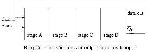
We make provisions for loading data into the parallel-in/ serial-out shift register configured as a ring counter below. Any random pattern may be loaded. The most generally useful pattern is a single 1.

Loading binary 1000 into the ring counter, above, prior to shifting yields a viewable pattern. The data pattern for a single stage repeats every four clock pulses in our 4-stage example. The waveforms for all four stages look the same, except for the one clock time delay from one stage to the next. See figure below.
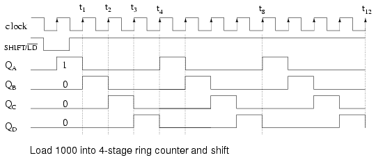
The circuit above is a divide by 4 counter. Comparing the clock input to any one of the outputs, shows a frequency ratio of 4:1. How may stages would we need for a divide by 10 ring counter? Ten stages would recirculate the 1 every 10 clock pulses.

An alternate method of initializing the ring counter to 1000 is shown above. The shift waveforms are identical to those above, repeating every fourth clock pulse. The requirement for initialization is a disadvantage of the ring counter over a conventional counter. At a minimum, it must be initialized at power-up since there is no way to predict what state flip-flops will power up in. In theory, initialization should never be required again. In actual practice, the flip-flops could eventually be corrupted by noise, destroying the data pattern. A "self correcting" counter, like a conventional synchronous binary counter would be more reliable.
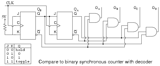
The above binary synchronous counter needs only two stages, but requires decoder gates. The ring counter had more stages, but was self decoding, saving the decode gates above. Another disadvantage of the ring counter is that it is not "self starting". If we need the decoded outputs, the ring counter looks attractive, in particular, if most of the logic is in a single shift register package. If not, the conventional binary counter is less complex without the decoder.

The waveforms decoded from the synchronous binary counter are identical to the previous ring counter waveforms. The counter sequence is (QA QB) = (00 01 10 11).
Johnson counters
The switch-tail ring counter, also know as the Johnson counter, overcomes some of the limitations of the ring counter. Like a ring counter a Johnson counter is a shift register fed back on its' self. It requires half the stages of a comparable ring counter for a given division ratio. If the complement output of a ring counter is fed back to the input instead of the true output, a Johnson counter results. The difference between a ring counter and a Johnson counter is which output of the last stage is fed back (Q or Q'). Carefully compare the feedback connection below to the previous ring counter.

This "reversed" feedback connection has a profound effect upon the behavior of the otherwise similar circuits. Recirculating a single 1 around a ring counter divides the input clock by a factor equal to the number of stages. Whereas, a Johnson counter divides by a factor equal to twice the number of stages. For example, a 4-stage ring counter divides by 4. A 4-stage Johnson counter divides by 8.
Start a Johnson counter by clearing all stages to 0s before the first clock. This is often done at power-up time. Referring to the figure below, the first clock shifts three 0s from ( QA QB QC) to the right into ( QB QC QD). The 1 at QD' (the complement of Q) is shifted back into QA. Thus, we start shifting 1s to the right, replacing the 0s. Where a ring counter recirculated a single 1, the 4-stage Johnson counter recirculates four 0s then four 1s for an 8-bit pattern, then repeats.

The above waveforms illustrates that multi-phase square waves are generated by a Johnson counter. The 4-stage unit above generates four overlapping phases of 50% duty cycle. How many stages would be required to generate a set of three phase waveforms? For example, a three stage Johnson counter, driven by a 360 Hertz clock would generate three 120o phased square waves at 60 Hertz.
The outputs of the flop-flops in a Johnson counter are easy to decode to a single state. Below for example, the eight states of a 4-stage Johnson counter are decoded by no more than a two input gate for each of the states. In our example, eight of the two input gates decode the states for our example Johnson counter.

No matter how long the Johnson counter, only 2-input decoder gates are needed. Note, we could have used uninverted inputs to the AND gates by changing the gate inputs from true to inverted at the FFs, Q to Q', (and vice versa). However, we are trying to make the diagram above match the data sheet for the CD4022B, as closely as practical.

Above, our four phased square waves QA to QD are decoded to eight signals (G0 to G7) active during one clock period out of a complete 8-clock cycle. For example, G0 is active high when both QA and QD are low. Thus, pairs of the various register outputs define each of the eight states of our Johnson counter example.

Above is the more complete internal diagram of the CD4022B Johnson counter. See the manufacturers' data sheet for minor details omitted. The major new addition to the diagram as compared to previous figures is the disallowed state detector composed of the two NOR gates. Take a look at the inset state table. There are 8-permissible states as listed in the table. Since our shifter has four flip-flops, there are a total of 16-states, of which there are 8-disallowed states. That would be the ones not listed in the table.
In theory, we will not get into any of the disallowed states as long as the shift register is RESET before first use. However, in the "real world" after many days of continuous operation due to unforeseen noise, power line disturbances, near lightning strikes, etc, the Johnson counter could get into one of the disallowed states. For high reliability applications, we need to plan for this slim possibility. More serious is the case where the circuit is not cleared at power-up. In this case there is no way to know which of the 16-states the circuit will power up in. Once in a disallowed state, the Johnson counter will not return to any of the permissible states without intervention. That is the purpose of the NOR gates.
Examine the table for the sequence (QA QB QC) = (010). Nowhere does this sequence appear in the table of allowed states. Therefore (010) is disallowed. It should never occur. If it does, the Johnson counter is in a disallowed state, which it needs to exit to any allowed state. Suppose that (QA QB QC) = (010). The second NOR gate will replace QB = 1 with a 0 at the D input to FF QC. In other words, the offending 010 is replaced by 000. And 000, which does appear in the table, will be shifted right. There are may triple-0 sequences in the table. This is how the NOR gates get the Johnson counter out of a disallowed state to an allowed state.
Not all disallowed states contain a 010 sequence. However, after a few clocks, this sequence will appear so that any disallowed states will eventually be escaped. If the circuit is powered-up without a RESET, the outputs will be unpredictable for a few clocks until an allowed state is reached. If this is a problem for a particular application, be sure to RESET on power-up.
Johnson counter devices
A pair of integrated circuit Johnson counter devices with the output states decoded is available. We have already looked at the CD4017 internal logic in the discussion of Johnson counters. The 4000 series devices can operate from 3V to 15V power supplies. The the 74HC' part, designed for a TTL compatiblity, can operate from a 2V to 6V supply, count faster, and has greater output drive capability. For complete device data sheets, follow the links.
-
CD4017 Johnson counter with 10 decoded outputs
CD4022 Johnson counter with 8 decoded outputs
[*]
- 74HC4017 Johnson counter, 10 decoded outputs
[*]

The ANSI symbols for the modulo-10 (divide by 10) and modulo-8 Johnson counters are shown above. The symbol takes on the characteristics of a counter rather than a shift register derivative, which it is. Waveforms for the CD4022 modulo-8 and operation were shown previously. The CD4017B/ 74HC4017 decade counter is a 5-stage Johnson counter with ten decoded outputs. The operation and waveforms are similar to the CD4017. In fact, the CD4017 and CD4022 are both detailed on the same data sheet. See above links. The 74HC4017 is a more modern version of the decade counter.
These devices are used where decoded outputs are needed instead of the binary or BCD (Binary Coded Decimal) outputs found on normal counters. By decoded, we mean one line out of the ten lines is active at a time for the '4017 in place of the four bit BCD code out of conventional counters. See previous waveforms for 1-of-8 decoding for the '4022 Octal Johnson counter.
Practical applications

The above Johnson counter shifts a lighted LED each fifth of a second around the ring of ten. Note that the 74HC4017 is used instead of the '40017 because the former part has more current drive capability. From the data sheet, (at the link above) operating at VCC= 5V, the VOH= 4.6V at 4ma. In other words, the outputs can supply 4 ma at 4.6 V to drive the LEDs. Keep in mind that LEDs are normally driven with 10 to 20 ma of current. Though, they are visible down to 1 ma. This simple circuit illustrates an application of the 'HC4017. Need a bright display for an exhibit? Then, use inverting buffers to drive the cathodes of the LEDs pulled up to the power supply by lower value anode resistors.
The 555 timer, serving as an astable multivibrator, generates a clock frequency determined by R1 R2 C1. This drives the 74HC4017 a step per clock as indicated by a single LED illuminated on the ring. Note, if the 555 does not reliably drive the clock pin of the '4015, run it through a single buffer stage between the 555 and the '4017. A variable R2 could change the step rate. The value of decoupling capacitor C2 is not critical. A similar capacitor should be applied across the power and ground pins of the '4017.

The Johnson counter above generates 3-phase square waves, phased 60o apart with respect to (QA QB QC). However, we need 120o phased waveforms of power applications (see Volume II, AC). Choosing P1=QA P2=QC P3=QB' yields the 120o phasing desired. See figure below. If these (P1 P2 P3) are low-pass filtered to sine waves and amplified, this could be the beginnings of a 3-phase power supply. For example, do you need to drive a small 3-phase 400 Hz aircraft motor? Then, feed 6x 400Hz to the above circuit CLOCK. Note that all these waveforms are 50% duty cycle.

The circuit below produces 3-phase nonoverlapping, less than 50% duty cycle, waveforms for driving 3-phase stepper motors.

Above we decode the overlapping outputs QA QB QC to non-overlapping outputs P0 P1 P2 as shown below. These waveforms drive a 3-phase stepper motor after suitable amplification from the milliamp level to the fractional amp level using the ULN2003 drivers shown above, or the discrete component Darlington pair driver shown in the circuit which follow. Not counting the motor driver, this circuit requires three IC (Integrated Circuit) packages: two dual type "D" FF packages and a quad NAND gate.


A single CD4017, above, generates the required 3-phase stepper waveforms in the circuit above by clearing the Johnson counter at count 3. Count 3 persists for less than a microsecond before it clears its' self. The other counts (Q0=G0 Q1=G1 Q2=G2) remain for a full clock period each.
The Darlington bipolar transistor drivers shown above are a substitute for the internal circuitry of the ULN2003. The design of drivers is beyond the scope of this digital electronics chapter. Either driver may be used with either waveform generator circuit.

The above waceforms make the most sense in the context of the internal logic of the CD4017 shown earlier in this section. Though, the AND gating equations for the internal decoder are shown. The signals QA QB QC are Johnson counter direct shift register outputs not available on pin-outs. The QD waveform shows resetting of the '4017 every three clocks. Q0 Q1 Q2, etc. are decoded outputs which actually are available at output pins.

Above we generate waveforms for driving a unipolar stepper motor, which only requires one polarity of driving signal. That is, we do not have to reverse the polarity of the drive to the windings. This simplifies the power driver between the '4017 and the motor. Darlington pairs from a prior diagram may be substituted for the ULN3003.

Once again, the CD4017B generates the required waveforms with a reset after the teminal count. The decoded outputs Q0 Q1 Q2 Q3 sucessively drive the stepper motor windings, with Q4 reseting the counter at the end of each group of four pulses.

No comments:
Post a Comment
Please give valuable comments on this post.