
The final transistor amplifier configuration we need to study is the common-base. This configuration is more complex than the other two, and is less common due to its strange operating characteristics.
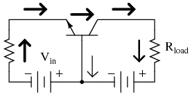
It is called the common-base configuration because (DC power source aside), the signal source and the load share the base of the transistor as a common connection point:

Perhaps the most striking characteristic of this configuration is that the input signal source must carry the full emitter current of the transistor, as indicated by the heavy arrows in the first illustration. As we know, the emitter current is greater than any other current in the transistor, being the sum of base and collector currents. In the last two amplifier configurations, the signal source was connected to the base lead of the transistor, thus handling the least current possible.
Because the input current exceeds all other currents in the circuit, including the output current, the current gain of this amplifier is actually less than 1 (notice how Rload is connected to the collector, thus carrying slightly less current than the signal source). In other words, it attenuates current rather than amplifying it. With common-emitter and common-collector amplifier configurations, the transistor parameter most closely associated with gain was β. In the common-base circuit, we follow another basic transistor parameter: the ratio between collector current and emitter current, which is a fraction always less than 1. This fractional value for any transistor is called the alpha ratio, or α ratio.
Since it obviously can't boost signal current, it only seems reasonable to expect it to boost signal voltage. A SPICE simulation will vindicate that assumption:

common-base amplifier
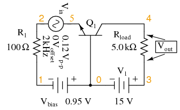
vin 0 1
r1 1 2 100
q1 4 0 2 mod1
v1 3 0 dc 15
rload 3 4 5k
.model mod1 npn
.dc vin 0.6 1.2 .02
.plot dc v(3,4)
.end

Notice how in this simulation the output voltage goes from practically nothing (cutoff) to 15.75 volts (saturation) with the input voltage being swept over a range of 0.6 volts to 1.2 volts. In fact, the output voltage plot doesn't show a rise until about 0.7 volts at the input, and cuts off (flattens) at about 1.12 volts input. This represents a rather large voltage gain with an output voltage span of 15.75 volts and an input voltage span of only 0.42 volts: a gain ratio of 37.5, or 31.48 dB. Notice also how the output voltage (measured across Rload) actually exceeds the power supply (15 volts) at saturation, due to the series-aiding effect of the the input voltage source.
A second set of SPICE analyses with an AC signal source (and DC bias voltage) tells the same story: a high voltage gain.
common-base amplifier
vin 5 2 sin (0 0.12 2000 0 0)
vbias 0 1  dc 0.95
r1 2 1 100
q1 4 0 5 mod1
v1 3 0 dc 15
rload 3 4 5k
.model mod1 npn
.tran 0.02m 0.78m
.plot tran v(5,2) v(4,3)
.end

No comments:
Post a Comment
Please give valuable comments on this post.