
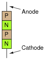
Our exploration of thyristors begins with a device called the four-layer diode, also known as a PNPN diode, or a Shockley diode after its inventor, William Shockley. This is not to be confused with a Schottky diode, that two-layer metal-semiconductor device known for its high switching speed. A crude illustration of the Shockley diode, often seen in textbooks, is a four-layer sandwich of P-N-P-N semiconductor material:
Unfortunately, this simple illustration does nothing to enlighten the viewer on how it works or why. Consider an alternative rendering of the device's construction:
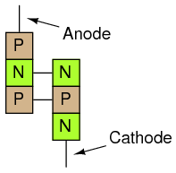
Shown like this, it appears to be a set of interconnected bipolar transistors, one PNP and the other NPN. Drawn using standard schematic symbols, and respecting the layer doping concentrations not shown in the last image, the Shockley diode looks like this:

Let's connect one of these devices to a source of variable voltage and see what happens:

With no voltage applied, of course there will be no current. As voltage is initially increased, there will still be no current because neither transistor is able to turn on: both will be in cutoff mode. To understand why this is, consider what it takes to turn a bipolar junction transistor on: current through the base-emitter junction. As you can see in the diagram, base current through the lower transistor is controlled by the upper transistor, and the base current through the upper transistor is controlled by the lower transistor. In other words, neither transistor can turn on until the other transistor turns on. What we have here, in vernacular terms, is known as a Catch-22.
So how can a Shockley diode ever conduct current, if its constituent transistors stubbornly maintain themselves in a state of cutoff? The answer lies in the behavior of real transistors as opposed to ideal transistors. An ideal bipolar transistor will never conduct collector current if there is no base current, no matter how much or little voltage we apply between collector and emitter. Real transistors, on the other hand, have definite limits to how much collector-emitter voltage they can withstand before they break down and conduct. If two real transistors are connected together in this fashion to form a Shockley diode, they will be able to conduct if there is sufficient voltage applied by the battery between anode and cathode to cause one of them to break down. Once one transistor breaks down and begins to conduct, it will allow base current through the other transistor, causing it to turn on in a normal fashion, which then allows base current through the first transistor. The end result is that both transistors will be saturated, now keeping each other turned on instead of off.
So, we can force a Shockley diode to turn on by applying sufficient voltage between anode and cathode. As we have seen, this will inevitably cause one of the transistors to turn on, which then turns the other transistor on, ultimately "latching" both transistors on where they will tend to remain. But how do we now get the two transistors to turn off again? Even if the applied voltage is reduced to a point well below what it took to get the Shockley diode conducting, it will remain conducting because both transistors now have base current to maintain regular, controlled conduction. The answer to this is to reduce the applied voltage to a much lower point where there is too little current to maintain transistor bias, at which point one of the transistors will cutoff, which then halts base current through the other transistor, sealing both transistors in the "off" state as they were before any voltage was applied at all.
If we graph this sequence of events and plot the results on an I/V graph, the hysteresis is very evident. First, we will observe the circuit as the DC voltage source (battery) is set to zero voltage:

Next, we will steadily increase the DC voltage. Current through the circuit is at or nearly at zero, as the breakdown limit has not been reached for either transistor:

When the voltage breakdown limit of one transistor is reached, it will begin to conduct collector current even though no base current has gone through it yet. Normally, this sort of treatment would destroy a bipolar junction transistor, but the PNP junctions comprising a Shockley diode are engineered to take this kind of abuse, similar to the way a Zener diode is built to handle reverse breakdown without sustaining damage. For the sake of illustration I'll assume the lower transistor breaks down first, sending current through the base of the upper transistor:

As the upper transistor receives base current, it turns on as expected. This action allows the lower transistor to conduct normally, the two transistors "sealing" themselves in the "on" state. Full current is very quickly seen in the circuit:

The positive feedback mentioned earlier in this chapter is clearly evident here. When one transistor breaks down, it allows current through the device structure. This current may be viewed as the "output" signal of the device. Once an output current is established, it works to hold both transistors in saturation, thus ensuring the continuation of a substantial output current. In other words, an output current "feeds back" positively to the input (transistor base current) to keep both transistors in the "on" state, thus reinforcing (or regenerating) itself.
With both transistors maintained in a state of saturation with the presence of ample base current, they will continue to conduct even if the applied voltage is greatly reduced from the breakdown level. The effect of positive feedback is to keep both transistors in a state of saturation despite the loss of input stimulus (the original, high voltage needed to break down one transistor and cause a base current through the other transistor):

If the DC voltage source is turned down too far, though, the circuit will eventually reach a point where there isn't enough current to sustain both transistors in saturation. As one transistor passes less and less collector current, it reduces the base current for the other transistor, thus reducing base current for the first transistor. The vicious cycle continues rapidly until both transistors fall into cutoff:

Here, positive feedback is again at work: the fact that the cause/effect cycle between both transistors is "vicious" (a decrease in current through one works to decrease current through the other, further decreasing current through the first transistor) indicates a positive relationship between output (controlled current) and input (controlling current through the transistors' bases).
The resulting curve on the graph is classicly hysteretic: as the input signal (voltage) is increased and decreased, the output (current) does not follow the same path going down as it did going up:

Put in simple terms, the Shockley diode tends to stay on once it's turned on, and stay off once it's turned off. There is no "in-between" or "active" mode in its operation: it is a purely on or off device, as are all thyristors.
There are a few special terms applied to Shockley diodes and all other thyristor devices built upon the Shockley diode foundation. First is the term used to describe its "on" state: latched. The word "latch" is reminiscent of a door lock mechanism, which tends to keep the door closed once it has been pushed shut. The term firing refers to the initiation of a latched state. In order to get a Shockley diode to latch, the applied voltage must be increased until breakover is attained. Despite the fact that this action is best described in terms of transistor breakdown, the term breakover is used instead because the end result is a pair of transistors in mutual saturation rather than destruction as would be the case with a normal transistor. A latched Shockley diode is re-set back into its nonconducting state by reducing current through it until low-current dropout occurs.
It should be noted that Shockley diodes may be fired in a way other than breakover: excessive voltage rise, or dv/dt. This is when the applied voltage across the diode increases at a high rate of change. This is able to cause latching (turning on) of the diode due to inherent junction capacitances within the transistors. Capacitors, as you may recall, oppose changes in voltage by drawing or supplying current. If the applied voltage across a Shockley diode rises at too fast a rate, those tiny capacitances will draw enough current during that time to activate the transistor pair, turning them both on. Usually, this form of latching is undesirable, and can be minimized by filtering high-frequency (fast voltage rises) from the diode with series inductors and/or parallel resistor-capacitor networks called snubbers:

The voltage rise limit of a Shockley diode is referred to as the critical rate of voltage rise. Manufacturers usually provide this specification for the devices they sell.
- REVIEW:
- Shockley diodes are four-layer PNPN semiconductor devices. They behave as a pair of interconnected PNP and NPN transistors.
- Like all thyristors, Shockley diodes tend to stay on once they've been turned on (latched), and stay off once they've been turned off.
- There are two ways to latch a Shockley diode: exceed the anode-to-cathode breakover voltage, or exceed the anode-to-cathode critical rate of voltage rise.
- There is only one way to cause a Shockley diode to stop conducting, and that is to reduce the current going through it to a level below its low-current dropout threshold.

No comments:
Post a Comment
Please give valuable comments on this post.